Page 1 of 1
Copper filling for PCB or not ?
Posted: 17 Oct 2020, 18:40
by Grumpf
I'm designing some PCBs for various projects. I heard in the EasyEDA tutorial that you may or may not want to fill empty areas with copper to your board as it may create interference for radio devices.
Anyone has an advice about that ? What's best practice ?
Thanks !
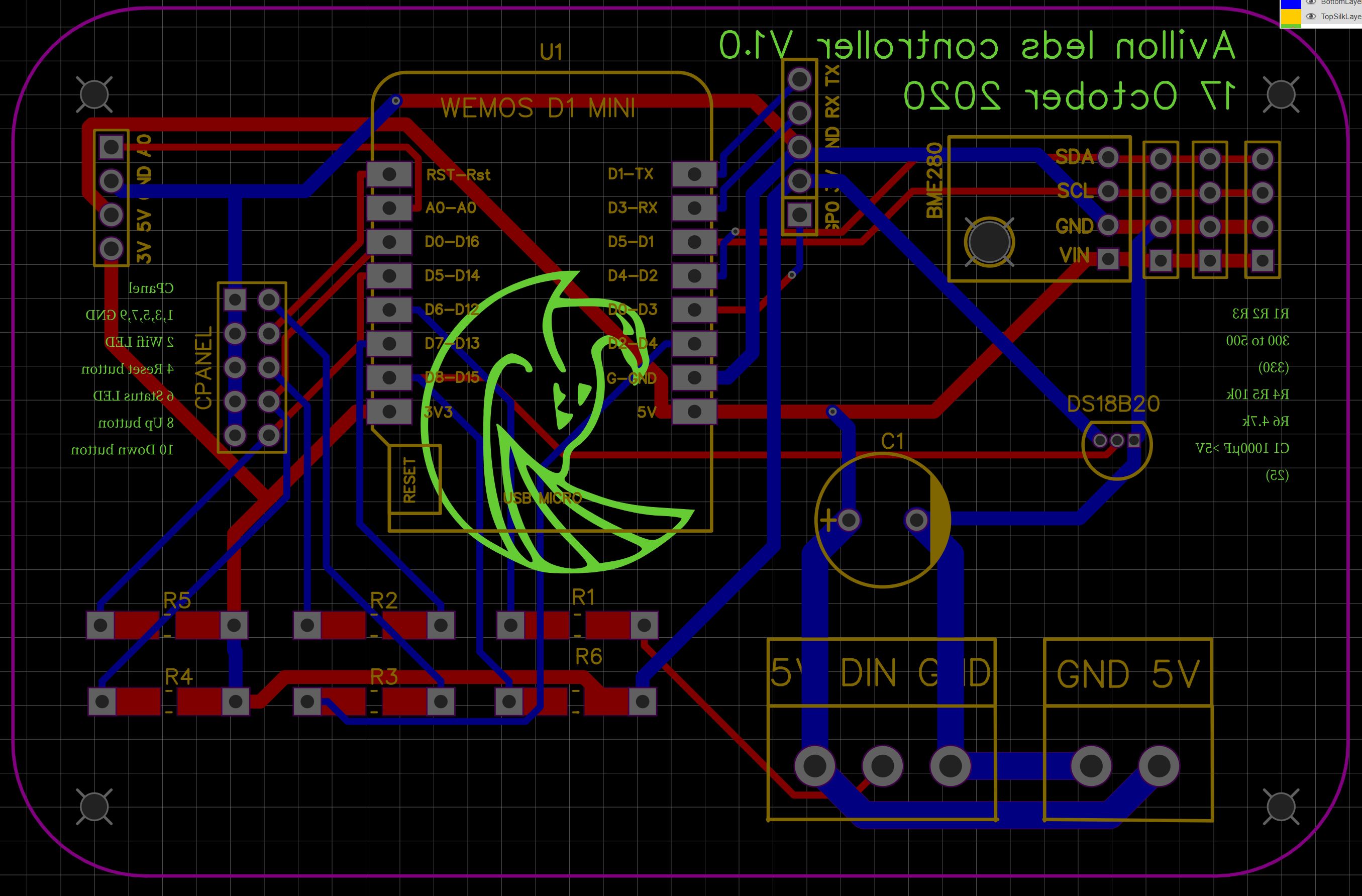
- WithoutCopper.jpg (550.01 KiB) Viewed 12404 times

- Copper.jpg (442.75 KiB) Viewed 12404 times
Re: Copper filling for PCB or not ?
Posted: 17 Oct 2020, 21:02
by TD-er
I always try to use one side for the GND and one for the power line that's most used.
So the copper pour then also acts as a (much) wider track, but more importantly you have a higher chance the return current has room to follow its preferred path.
Just some info on the return current.
With frequencies above a few 100 kHz, the return current of a trace will follow the feeding trace.
So imagine a ground plane filling the entire bottom side with a trace on the other side.
If you enter a signal with a frequency over a few 100 kHz, then the return current on the ground plane is following the trace on the other side. (so it is not taking the shortest path as you maybe would expect)
So by having the Vcc and GND on each side connected with the copper pour you have a greater chance the return current can follow the track on the opposite side.
This also allows to reduce crosstalk between signals. (still no magic rule, but it may help a bit)
Re: Copper filling for PCB or not ?
Posted: 18 Oct 2020, 09:03
by Grumpf
Thank you. That's way above my level but I'll TLDR you (yes yes, probably done millions of time) and use one side for GND and the other for 3.3V then.
Have a nice day sir, it's a hard time for a consultant like me being covided home but I've joined your patreon.
Re: Copper filling for PCB or not ?
Posted: 18 Oct 2020, 20:44
by TD-er
If you would like to see more about the effects of the "return current", you can see this very interesting video about it:
https://www.youtube.com/watch?v=4nEd1jT ... ertFeranec
Re: Copper filling for PCB or not ?
Posted: 19 Oct 2020, 13:36
by Grumpf
Thank you. I wanted to kill him when he said : "But I'm not going to show you the results yet, first let's check how I arrived at this design." Something similar.
Very informative, way above my level but now I know. I ordered the PCBs, let's cross fingers !
Re: Copper filling for PCB or not ?
Posted: 19 Oct 2020, 15:37
by TD-er
Well lots of things are also above my level, but once you've heard about things it still keeps wondering around in your mind and some day it may be useful

I know a colleague of mine told me this about the path of return currents years ago and I was like sure that's nice to know when working with GHz speeds..
But it appears to be happening even at the speeds we can software toggle in the ESP, so it can make a difference even in our "low frequency" applications.
So by using large copper pour planes attached to either GND or Vcc, you can already mitigate some of these issues, without even having to fully understand them.
As soon as you run into crosstalk of signals at few MHz frequencies, you know where to start looking now and then you also realize you're at the next level
Re: Copper filling for PCB or not ?
Posted: 19 Oct 2020, 22:14
by chemmex
You should definitely cut off the copper in front of the antenna area of Wemos at both sides of the PCB. And leave some extra room
Re: Copper filling for PCB or not ?
Posted: 19 Oct 2020, 23:42
by TD-er
Woops, yes that one I missed.
I'm using the ESP07S myself on my boards, so those don't have the PCB antenna but have an IPEX connector for an external antenna.
You could still go for the Wemos boards that also have such an antenna connector.
Just be aware if you need to move a 0 Ohm resistor to switch between PCB or IPEX antenna. (located near the IPEX connector)
Re: Copper filling for PCB or not ?
Posted: 20 Oct 2020, 08:06
by Grumpf
Thanks all. I didn't do that but fortunately I was already planning on using a D1 mini pro as the device will be inside a wall.
Cheers and thanks for the tip, next board I'll cut.